

- Open Access
Quantum Transport in Bismuth Two-Dimensional Electron System
Phys. Rev. X 15, 041047 – Published 9 December, 2025
DOI: https://doi.org/10.1103/hptx-pw9s
Abstract
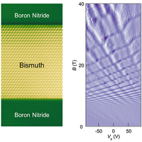
Two-dimensional electron systems (2DESs) have represented an ever-expanding frontier in condensed matter physics. Over the past two decades, this growth has primarily been propelled by the emergence of novel 2DESs, exemplified by graphene and other two-dimensional (2D) crystals, each exhibiting distinctive properties. In this study, we synthesize high-quality -phase bismuth thin films on exfoliated hexagonal boron nitride (hBN) and establish that bismuth surface states form a high-mobility 2DES with strong spin-orbit coupling (SOC). The extreme two dimensionality of the 2DES is characterized by an out-of-plane to in-plane effective-mass-anisotropy lower bound exceeding . We further demonstrate that the spin degeneracy of the hole pockets is completely lifted, providing unambiguous transport evidence that they originate from Rashba states induced by strong SOC in the bismuth thin film. Under magnetic fields up to 40 Tesla, electrostatic gating drives the carriers into the lowest Landau levels, revealing signatures of rotational symmetry breaking and electronic nematicity. These findings position the bismuth 2DES as a compelling platform for exploring topological quantum phenomena in systems with strong SOC and high carrier mobility.
Physics Subject Headings (PhySH)
- Landau levels
- Quantum transport
- Shubnikov-de Haas effect
- Surface states
- Hexagonal boron nitride
- Layered crystals
- Semimetals
- Surfaces
- Two-dimensional electron system
- Ultrathin films
- Annealing
- Atomic force microscopy
- Density functional theory
- High-resolution transmission electron microscopy
- Molecular beam epitaxy
- Scanning tunneling microscopy
- Transport techniques
Collections
This article appears in the following collection:

Special Collection on 2D Materials
PRX launches this collection to showcase articles in the exciting field of 2D materials and van der Waals heterostructures to constitute an emblematic example of the diversity of physics in this very active scientific domain.
Popular Summary
Bismuth is an exceptional material for creating 2D electron systems. It combines high electrical mobility with one of the strongest spin-orbit couplings of any nonradioactive element. This coupling can split electron states according to their spin direction. But creating high-quality 2D bismuth systems is challenging because the bulk material resists being peeled into thin layers, and conventional growth techniques often produce films with unwanted structures or defects. We overcome these challenges and show that when bismuth is made into an ultrathin, high-quality film, the spin-split surface states dominate its behavior, forming a stable and highly mobile 2D system of electrons.
To achieve this, we grow atomically thin, single-crystal films of bismuth on sheets of hexagonal boron nitride using van der Waals epitaxy, a gentle method that avoids damaging the layers. Measurements of how electrons move in magnetic fields confirm that the films behave as nearly perfect 2D conductors. By adjusting the carrier concentration, we demonstrate that each electronic state carries only one spin orientation—clear evidence that the strong spin-orbit interaction in bismuth fully removes the usual spin pairing. When we apply very high magnetic fields, we also observe the electronic energy levels splitting further and the crystal’s rotational symmetry breaking, signs that strain or subtle electron alignment effects are influencing the system.
These findings establish ultrathin bismuth films as a playground for studying quantum behaviors that rely on strong spin-orbit effects. Because the spin splitting in bismuth is so large, such effects could potentially persist at higher temperatures than in most other materials, opening the door to realizing robust, spin-based quantum states useful for future electronic and quantum technologies.
Article Text
Supplemental Material
References (105)
- V. S. Édel’man, Electrons in bismuth, Adv. Phys. 25, 555 (1976).
- D. Shoenberg, Magnetic Oscillations in Metals (Cambridge University Press, Cambridge, England, 1984).
- N. W. Ashcroft and N. D. Mermin, Solid State Physics (Holt, Rinehart and Winston, New York, 1976).
- A. Brugmans, Antonii Brugmans Magnetismus, seu, De affinitatibus magneticis observationes academicæ (Apud Luzac & Van Damme, Leiden, 1778).
- A. v. Ettingshausen and W. Nernst, Ueber das Auftreten electromotorischer Kräfte in Metallplatten, welche von einem Wärmestrome durchflossen werden und sich im magnetischen Felde befinden, Ann. Phys. (Berlin) 265, 343 (1886).
- L. Shubnikov and W. J. de Haas, Magnetische Widerstandsvergrösserung in Einkristallen von Wismut bei tiefen Temperaturen, Proc. R. Neth. Acad. Arts Sci. 33, 130 (1930), https://dwc.knaw.nl/DL/publications/PU00014617.pdf.
- W. J. de Haas and P. M. van Alphen, The dependence of the susceptibility of diamagnetic metals upon the field, Proc. R. Neth. Acad. Arts Sci. 33, 1106 (1930), https://dwc.knaw.nl/DL/publications/PU00014621.pdf.
- X.-L. Qi and S.-C. Zhang, Topological insulators and superconductors, Rev. Mod. Phys. 83, 1057 (2011).
- B. Jäck, Y. Xie, J. Li, S. Jeon, B. A. Bernevig, and A. Yazdani, Observation of a Majorana zero mode in a topologically protected edge channel, Science 364, 1255 (2019).
- S. Ito et al., Proving nontrivial topology of pure bismuth by quantum confinement, Phys. Rev. Lett. 117, 236402 (2016).
- Y. Fukushima et al., Spin-polarized saddle points in the topological surface states of elemental bismuth revealed by pump-probe spin- and angle-resolved photoemission spectroscopy, Phys. Rev. B 110, L041401 (2024).
- B. E. Feldman, M. T. Randeria, A. Gyenis, F. Wu, H. Ji, R. J. Cava, A. H. MacDonald, and A. Yazdani, Observation of a nematic quantum Hall liquid on the surface of bismuth, Science 354, 316 (2016).
- K. Behnia, L. Balicas, and Y. Kopelevich, Signatures of electron fractionalization in ultraquantum bismuth, Science 317, 1729 (2007).
- L. Li, J. G. Checkelsky, Y. S. Hor, C. Uher, A. F. Hebard, R. J. Cava, and N. P. Ong, Phase transitions of Dirac electrons in bismuth, Science 321, 547 (2008).
- O. Prakash, A. Kumar, A. Thamizhavel, and S. Ramakrishnan, Evidence for bulk superconductivity in pure bismuth single crystals at ambient pressure, Science 355, 52 (2017).
- Z. Zhu, J. Wang, H. Zuo, B. Fauqué, R. D. McDonald, Y. Fuseya, and K. Behnia, Emptying Dirac valleys in bismuth using high magnetic fields, Nat. Commun. 8, 15297 (2017).
- F. Schindler et al., Higher-order topology in bismuth, Nat. Phys. 14, 918 (2018).
- J. Gou, H. Bai, X. Zhang, Y. L. Huang, S. Duan, A. Ariando, S. A. Yang, L. Chen, Y. Lu, and A. T. S. Wee, Two-dimensional ferroelectricity in a single-element bismuth monolayer, Nature (London) 617, 67 (2023).
- A. K. Geim, Nobel lecture: Random walk to graphene, Rev. Mod. Phys. 83, 851 (2011).
- K. S. Novoselov, Nobel lecture: Graphene: Materials in the flatland, Rev. Mod. Phys. 83, 837 (2011).
- T. Ando, A. B. Fowler, and F. Stern, Electronic properties of two-dimensional systems, Rev. Mod. Phys. 54, 437 (1982).
- K. v. Klitzing, G. Dorda, and M. Pepper, New method for high-accuracy determination of the fine-structure constant based on quantized Hall resistance, Phys. Rev. Lett. 45, 494 (1980).
- D. C. Tsui, H. L. Stormer, and A. C. Gossard, Two-dimensional magnetotransport in the extreme quantum limit, Phys. Rev. Lett. 48, 1559 (1982).
- K. S. Novoselov, A. K. Geim, S. V. Morozov, D. Jiang, Y. Zhang, S. V. Dubonos, I. V. Grigorieva, and A. A. Firsov, Electric field effect in atomically thin carbon films, Science 306, 666 (2004).
- K. S. Novoselov, A. K. Geim, S. V. Morozov, D. Jiang, M. I. Katsnelson, I. V. Grigorieva, S. V. Dubonos, and A. A. Firsov, Two-dimensional gas of massless Dirac fermions in graphene, Nature (London) 438, 197 (2005).
- Y. Zhang, Y.-W. Tan, H. L. Stormer, and P. Kim, Experimental observation of the quantum Hall effect and Berry’s phase in graphene, Nature (London) 438, 201 (2005).
- C. R. Dean et al., Boron nitride substrates for high-quality graphene electronics, Nat. Nanotechnol. 5, 722 (2010).
- K. F. Mak, C. Lee, J. Hone, J. Shan, and T. F. Heinz, Atomically thin : A new direct-gap semiconductor, Phys. Rev. Lett. 105, 136805 (2010).
- B. Radisavljevic, A. Radenovic, J. Brivio, V. Giacometti, and A. Kis, Single-layer transistors, Nat. Nanotechnol. 6, 147 (2011).
- L. Li, Y. Yu, G. J. Ye, Q. Ge, X. Ou, H. Wu, D. Feng, X. H. Chen, and Y. Zhang, Black phosphorus field-effect transistors, Nat. Nanotechnol. 9, 372 (2014).
- L. Li et al., Quantum Hall effect in black phosphorus two-dimensional electron system, Nat. Nanotechnol. 11, 593 (2016).
- C. Gong et al., Discovery of intrinsic ferromagnetism in two-dimensional van der Waals crystals, Nature (London) 546, 265 (2017).
- B. Huang et al., Layer-dependent ferromagnetism in a van der Waals crystal down to the monolayer limit, Nature (London) 546, 270 (2017).
- Y. Deng et al., Gate-tunable room-temperature ferromagnetism in two-dimensional , Nature (London) 563, 94 (2018).
- Y. Deng, Y. Yu, M. Z. Shi, Z. Guo, Z. Xu, J. Wang, X. H. Chen, and Y. Zhang, Quantum anomalous Hall effect in intrinsic magnetic topological insulator , Science 367, 895 (2020).
- Y. Yu, L. Ma, P. Cai, R. Zhong, C. Ye, J. Shen, G. D. Gu, X. H. Chen, and Y. Zhang, High-temperature superconductivity in monolayer , Nature (London) 575, 156 (2019).
- Y. Cao, V. Fatemi, S. Fang, K. Watanabe, T. Taniguchi, E. Kaxiras, and P. Jarillo-Herrero, Unconventional superconductivity in magic-angle graphene superlattices, Nature (London) 556, 43 (2018).
- H. Park et al., Observation of fractionally quantized anomalous Hall effect, Nature (London) 622, 74 (2023).
- Ph. Hofmann, The surfaces of bismuth: Structural, and electronic properties, Prog. Surf. Sci. 81, 191 (2006).
- S. Murakami, Quantum spin Hall effect and enhanced magnetic response by spin-orbit coupling, Phys. Rev. Lett. 97, 236805 (2006).
- C. Sabater, D. Gosálbez-Martínez, J. Fernández-Rossier, J. G. Rodrigo, C. Untiedt, and J. J. Palacios, Topologically protected quantum transport in locally exfoliated bismuth at room temperature, Phys. Rev. Lett. 110, 176802 (2013).
- K. Jiang, J. Ji, W. Gong, L. Ding, J. Li, P. Li, B. Li, and F. Geng, Mechanical cleavage of non-van der Waals structures towards two-dimensional crystals, Nat. Synth. 2, 58 (2023).
- O. Yu, R. Allgayer, S. Godin, J. Lalande, P. Fossati, C. Hsu, T. Szkopek, and G. Gervais, Method of mechanical exfoliation of bismuth with micro-trench structures, J. Appl. Phys. 134, 244302 (2023).
- F. Reis, G. Li, L. Dudy, M. Bauernfeind, S. Glass, W. Hanke, R. Thomale, J. Schäfer, and R. Claessen, Bismuthene on a substrate: A candidate for a high-temperature quantum spin Hall material, Science 357, 287 (2017).
- R. Stühler, A. Kowalewski, F. Reis, D. Jungblut, F. Dominguez, B. Scharf, G. Li, J. Schäfer, E. M. Hankiewicz, and R. Claessen, Effective lifting of the topological protection of quantum spin Hall edge states by edge coupling, Nat. Commun. 13, 3480 (2022).
- A. Fang, C. Adamo, S. Jia, R. J. Cava, S.-C. Wu, C. Felser, and A. Kapitulnik, Bursting at the seams: Rippled monolayer bismuth on , Sci. Adv. 4, eaaq0330 (2018).
- T. Hirahara, G. Bihlmayer, Y. Sakamoto, M. Yamada, H. Miyazaki, S. Kimura, S. Blügel, and S. Hasegawa, Interfacing 2D and 3D topological insulators: bilayer on , Phys. Rev. Lett. 107, 166801 (2011).
- M. Chen, J.-P. Peng, H.-M. Zhang, L.-L. Wang, K. He, X.-C. Ma, and Q.-K. Xue, Molecular beam epitaxy of bilayer films on topological insulator : A scanning tunneling microscopy study, Appl. Phys. Lett. 101, 081603 (2012).
- T. Nagao, J. T. Sadowski, M. Saito, S. Yaginuma, Y. Fujikawa, T. Kogure, T. Ohno, Y. Hasegawa, S. Hasegawa, and T. Sakurai, Nanofilm allotrope and phase transformation of ultrathin film on , Phys. Rev. Lett. 93, 105501 (2004).
- T. Nagao, S. Yaginuma, M. Saito, T. Kogure, J. T. Sadowski, T. Ohno, S. Hasegawa, and T. Sakurai, Strong lateral growth and crystallization via two-dimensional allotropic transformation of semi-metal film, Surf. Sci. 590, 247 (2005).
- H. Hirayama, Nucleation and growth of ultrathin films, Adv. Phys. X 6, 1845975 (2021).
- S. A. Scott, M. V. Kral, and S. A. Brown, A crystallographic orientation transition and early stage growth characteristics of thin films on HOPG, Surf. Sci. 587, 175 (2005).
- D. N. McCarthy, D. Robertson, P. J. Kowalczyk, and S. A. Brown, The effects of annealing and growth temperature on the morphologies of nanostructures on HOPG, Surf. Sci. 604, 1273 (2010).
- N. Hussain, T. Liang, Q. Zhang, T. Anwar, Y. Huang, J. Lang, K. Huang, and H. Wu, Ultrathin nanosheets with superior photoluminescence, Small 13, 1701349 (2017).
- L. Chen et al., Exceptional electronic transport and quantum oscillations in thin bismuth crystals grown inside van der Waals materials, Nat. Mater. 23, 741 (2024).
- J. Zhao et al., Realization of 2D metals at the ångström thickness limit, Nature (London) 639, 354 (2025).
- A. Koma, Van der Waals epitaxy—a new epitaxial growth method for a highly lattice-mismatched system, Thin Solid Films 216, 72 (1992).
- C. R. Ast and H. Höchst, Fermi surface of measured by photoemission spectroscopy, Phys. Rev. Lett. 87, 177602 (2001).
- Yu. M. Koroteev, G. Bihlmayer, J. E. Gayone, E. V. Chulkov, S. Blügel, P. M. Echenique, and Ph. Hofmann, Strong spin-orbit splitting on surfaces, Phys. Rev. Lett. 93, 046403 (2004).
- T. Hirahara, T. Nagao, I. Matsuda, G. Bihlmayer, E. V. Chulkov, Yu. M. Koroteev, P. M. Echenique, M. Saito, and S. Hasegawa, Role of spin-orbit coupling and hybridization effects in the electronic structure of ultrathin films, Phys. Rev. Lett. 97, 146803 (2006).
- Yu. M. Koroteev, G. Bihlmayer, E. V. Chulkov, and S. Blügel, First-principles investigation of structural and electronic properties of ultrathin films, Phys. Rev. B 77, 045428 (2008).
- S. Xiao, D. Wei, and X. Jin, thin film with insulating interior but metallic surfaces, Phys. Rev. Lett. 109, 166805 (2012).
- K. Zhu, L. Wu, X. Gong, S. Xiao, and X. Jin, Quantum transport in the surface states of epitaxial thin films, Phys. Rev. B 94, 121401 (2016).
- H. Du et al., Surface Landau levels and spin states in bismuth (111) ultrathin films, Nat. Commun. 7, 10814 (2016).
- A. G. F. Garcia, M. Neumann, F. Amet, J. R. Williams, K. Watanabe, T. Taniguchi, and D. Goldhaber-Gordon, Effective cleaning of hexagonal boron nitride for graphene devices, Nano Lett. 12, 4449 (2012).
- Y. Yang, K. Xu, L. N. Holtzman, K. Yang, K. Watanabe, T. Taniguchi, J. Hone, K. Barmak, and M. R. Rosenberger, Atomic defect quantification by lateral force microscopy, ACS Nano 18, 6887 (2024).
- S. Yaginuma, T. Nagao, J. T. Sadowski, A. Pucci, Y. Fujikawa, and T. Sakurai, Surface pre-melting and surface flattening of nanofilms on , Surf. Sci. 547, L877 (2003).
- See Supplemental Material at http://link.aps.org/supplemental/10.1103/hptx-pw9s, which includes Refs. [69–80], for additional data and analyses about AFM, STM, and STEM characterization of and heterostructures, magnetotransport and quantum oscillations observed in and heterostructures, and DFT electronic structure of the bismuth thin film (n.d.).
- Z. Jiang, V. Soghomonian, and J. J. Heremans, Carrier properties of grown on mica and , Phys. Rev. Mater. 6, 095003 (2022).
- R. Ushioda, M. Shimura, K. Nakatsuji, and H. Hirayama, Growth-rate dependence of the structural transition of bismuth islands on substrates, Phys. Rev. Mater. 6, 043403 (2022).
- Y. Pan et al., Heteroepitaxy of semiconducting thin films on arbitrary surfaces for large-scale heterogeneous integration, Nat. Synth. 1, 701 (2022).
- S. Y. F. Zhao et al., Time-reversal symmetry breaking superconductivity between twisted cuprate superconductors, Science 382, 1422 (2023).
- S. Guo et al., An ultra-high vacuum system for fabricating clean two-dimensional material devices, Rev. Sci. Instrum. 94, 013903 (2023).
- D. Abdelbarey, J. Koch, Z. Mamiyev, C. Tegenkamp, and H. Pfnür, Thickness-dependent electronic transport through epitaxial nontrivial quantum films, Phys. Rev. B 102, 115409 (2020).
- Z. Zhu, B. Fauqué, K. Behnia, and Y. Fuseya, Magnetoresistance and valley degree of freedom in bulk bismuth, J. Phys. Condens. Matter 30, 313001 (2018).
- S. Zhang, Q. Wu, Y. Liu, and O. V. Yazyev, Magnetoresistance from Fermi surface topology, Phys. Rev. B 99, 035142 (2019).
- S. Zhang, Z. Liu, H. Pi, Z. Fang, H. Weng, and Q. Wu, Complex field-, temperature-, and angle-dependent Hall effects from intrinsic Fermi surface revealed by first-principles calculations, Phys. Rev. B 110, 205132 (2024).
- M. N. Ali et al., Large, non-saturating magnetoresistance in , Nature (London) 514, 205 (2014).
- A. B. Pippard, Magnetoresistance in Metals (Cambridge University Press, Cambridge, England, 1989).
- M. Aitani, T. Hirahara, S. Ichinokura, M. Hanaduka, D. Shin, and S. Hasegawa, In situ Magnetotransport measurements in ultrathin films: Evidence for surface-bulk coherent transport, Phys. Rev. Lett. 113, 206802 (2014).
- G. M. Minkov, O. E. Rut, A. A. Sherstobitov, S. A. Dvoretski, N. N. Mikhailov, and A. V. Germanenko, Quantum oscillations of transport coefficients and capacitance: A manifestation of the spin Hall effect, Phys. Rev. B 108, 075301 (2023).
- S. Datta, Electronic Transport in Mesoscopic Systems (Cambridge University Press, Cambridge, England, 1997).
- L. Onsager, Interpretation of the de Haas-van Alphen effect, London Edinburgh Dublin Phil. Mag. J. Sci. 43, 1006 (1952).
- L. Li et al., Quantum oscillations in a two-dimensional electron gas in black phosphorus thin films, Nat. Nanotechnol. 10, 608 (2015).
- P. Streda, Theory of quantised Hall conductivity in two dimensions, J. Phys. C 15, L717 (1982).
- V. Pudalov, S. Semenchinskii, and V. Edel’man, Oscillations of the chemical potential and the energy spectrum of electrons in the inversion layer at a silicon surface in a magnetic field, Sov. Phys. JETP 62, 1079 (1985), http://jetp.ras.ru/cgi-bin/dn/e_062_05_1079.pdf.
- C. H. W. Barnes, D. R. Mace, G. Faini, D. Mailly, M. Y. Simmons, C. J. B. Ford, and M. Pepper, Detection of the oscillation of the Fermi energy of a 2DEG, Surf. Sci. 361–362, 608 (1996).
- A. G. Davies, C. H. W. Barnes, K. R. Zolleis, J. T. Nicholls, M. Y. Simmons, and D. A. Ritchie, Hybridization of single- and double-layer behavior in a double-quantum-well structure, Phys. Rev. B 54, R17331 (1996).
- C. Ellenberger, B. Simovič, R. Leturcq, T. Ihn, S. E. Ulloa, K. Ensslin, D. C. Driscoll, and A. C. Gossard, Two-subband quantum Hall effect in parabolic quantum wells, Phys. Rev. B 74, 195313 (2006).
- C. A. Duarte, G. M. Gusev, A. A. Quivy, T. E. Lamas, A. K. Bakarov, and J. C. Portal, Landau-level crossing in two-subband systems in a tilted magnetic field, Phys. Rev. B 76, 075346 (2007).
- M. Karalic, C. Mittag, S. Mueller, T. Tschirky, W. Wegscheider, K. Ensslin, T. Ihn, and L. Glazman, Phase slips and parity jumps in quantum oscillations of inverted quantum wells, Phys. Rev. B 99, 201402 (2019).
- J. Ziegler, D. A. Kozlov, N. N. Mikhailov, S. Dvoretsky, and D. Weiss, Quantum Hall effect and Landau levels in the three-dimensional topological insulator , Phys. Rev. Res. 2, 033003 (2020).
- https://cstr.cn/31125.02.SHMFF.HM.
- F. F. Fang and P. J. Stiles, Effects of a tilted magnetic field on a two-dimensional electron gas, Phys. Rev. 174, 823 (1968).
- James G. Analytis, R. D. McDonald, S. C. Riggs, J.-H. Chu, G. S. Boebinger, and I. R. Fisher, Two-dimensional surface state in the quantum limit of a topological insulator, Nat. Phys. 6, 960 (2010).
- S. Xu et al., Odd-integer quantum Hall states and giant spin susceptibility in -type few-layer , Phys. Rev. Lett. 118, 067702 (2017).
- G. E. Smith, G. A. Baraff, and J. M. Rowell, Effective factor of electrons and holes in bismuth, Phys. Rev. 135, A1118 (1964).
- R. D. Brown, Shubnikov-de Haas measurements in bismuth, Phys. Rev. B 2, 928 (1970).
- Y. Liu and R. E. Allen, Electronic structure of the semimetals and , Phys. Rev. B 52, 1566 (1995).
- J. M. Schneider, B. A. Piot, I. Sheikin, and D. K. Maude, Using the de Haas–van Alphen effect to map out the closed three-dimensional Fermi surface of natural graphite, Phys. Rev. Lett. 108, 117401 (2012).
- B. Fallahazad, H. C. P. Movva, K. Kim, S. Larentis, T. Taniguchi, K. Watanabe, S. K. Banerjee, and E. Tutuc, Shubnikov-de Haas oscillations of high-mobility holes in monolayer and bilayer : Landau level degeneracy, effective mass, and negative compressibility, Phys. Rev. Lett. 116, 086601 (2016).
- G. Kresse and J. Furthmüller, Efficient iterative schemes for ab initio total-energy calculations using a plane-wave basis set, Phys. Rev. B 54, 11169 (1996).
- P. E. Blöchl, Projector augmented-wave method, Phys. Rev. B 50, 17953 (1994).
- J. P. Perdew, K. Burke, and M. Ernzerhof, Generalized gradient approximation made simple, Phys. Rev. Lett. 77, 3865 (1996).
- S. Grimme, J. Antony, S. Ehrlich, and H. Krieg, A consistent and accurate ab initio parametrization of density functional dispersion correction (DFT-D) for the 94 elements , J. Chem. Phys. 132, 154104 (2010).

